UAH team’s new technique protects data on solid-state drives from radiation

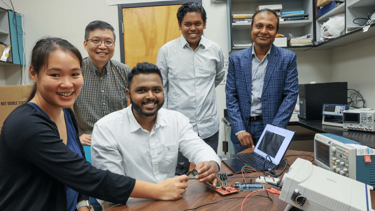
Dr. Biswajit Ray, right, with students (from left) Matchima Buddhanoy, Sijay Huang, Umeshwarnath Surendranathan and Mondol Anik Kumar in the Ray Research Group lab.
A new method of radiation-resistant computer data storage called watermark storage that’s been developed by a University of Alabama in Huntsville (UAH) professor leading a student team has direct applications in the nuclear power and space industries.
“Data-driven analytics are growing exponentially for space and nuclear environments,” says Dr. Biswajit Ray, an assistant professor of electrical and computer engineering at UAH, a part of the University of Alabama System.
He says the new storage system doesn’t rely on an electronic charge for NAND flash storage, as traditional data drives do. NAND stands for the “not and” type of flash memory, which is in common use. Interestingly, the watermark storage method requires no new components.
“We adeptly use the breakdown mechanism of a transistor’s oxide layer to imprint information on the same commercial off-the-shelf memory cells,” Dr. Ray says. “This technique is more resistant to irradiation damage compared to the traditional charge-based technique.”
He’s been working with Kannan Grant, director of UAH’s Office of Technology Commercialization, on a pending patent for the new technology.
Radiation tolerance is typically characterized as cumulative total dose, as expressed in units of rad(Si). So, how radiation tolerant is watermark data storage?
“We have tested the chips up to 100 krad(Si) and we find clear benefits using our method compared to the traditional charge based method,” Dr. Ray says. Just one krad is 1,000 rads, a strong enough radiation dose to kill a person.
“Our method shows a linear response of the bit error rate with a total dose, whereas the traditional method shows an exponential rise,” he says.
While much less data is lost in radioactive environments with the watermark technique, there is a downside. Data writing time is slower than traditional electronic storage, but Dr. Ray says that some of that downside can be minimized if NAND chip manufacturers allow a few additional operations on their chips.
“Writing time for traditional NAND flash media is roughly a few milliseconds per 16kB page, whereas imprinting time in our proposal will be a few seconds,” he says. “So, data writing time will increase by about 1,000 times. However, the proposed technique targets those applications where writing will be done only once and hence it will not be a significant bottleneck.”
Dr. Ray’s electrical and computer engineering student team members in the Ray Research Group, and the co-authors of the resulting research paper, are Matchima Buddhanoy, a doctoral student and the lead author; Sadman Sakib, a recent doctoral graduate now working at Intel; and Umeshwarnath Surendranathan, a doctoral student.
Collaborators and co-authors are Dr. Aleksandar Milenković, a UAH professor of electrical and computer engineering, and Dr. Maryla Wasiolek and Dr. Khalid Hattar, principal members of the technical staff at Sandia National Laboratories in Albuquerque, N.M.
Sandia provided support with Cobalt-60 gamma irradiation sources and helped conduct the experiments. The collaboration was contractually supported in part by the U.S. Department of Energy’s Office of Nuclear Energy through its Idaho Operations Office.
Future research will be partially supported by Dr. Ray’s five-year, $650,000 National Science Foundation CAREER grant to create more resilient, durable and energy-efficient computer memory drives. The work will involve further radiation testing of the new technique, Dr. Ray says.
We would like to explore and test this technique for a very high radiation environment such as a total dose of more than 1 megarad(Si),” he says.
“At a very high total dose NAND peripheral circuits fail, making the chip non-functional. We plan to work with NAND manufacturers to build rad-hard NAND peripherals. We also plan to evaluate high-dose response by selective shielding of the peripherals.”
Contact
Dr. Biswajit Ray
256.824.5679
biswajit.ray@uah.edu
Jim Steele
256.824.2772
jim.steele@uah.edu
